In Human-Computer Interaction, multi-material 3D printing is increasingly recognized for its capacity to produce conductive interactive objects. While various fabrication techniques have emerged in this domain, achieving the integration of highly conductive 3D structures within printed objects continues to pose a significant technical hurdle. Our study introduces Intercircuit, a novel integrated technique developed explicitly for fabricating highly conductive interactive objects. This method employs multi-material printing to form unified components along with their embedded structures of lower conductivity, enhancing conductivity through targeted plating. Distinct from traditional multi-material printing and surface conductivity augmentation methods, the Intercircuit method facilitates the creation of complex 3D circuitry while ensuring superior conductivity. Furthermore, this study introduces a supportive design tool aimed at aiding users in crafting conductive frameworks. Moreover, the practical application of this method is further elucidated through a series of case studies.
Background
In interactive fabrication, multi-material 3D printing has made it possible to integrate circuits into printed objects, but existing methods still face two major limitations. One approach relies on conductive PLA to directly print complex 3D circuitry, yet the high material resistance and interlayer resistance usually restrict these circuits to low-load applications such as sensing or display. Another approach improves performance through low-melting-point metals, embedded copper wires, or surface-applied conductive materials, but these methods often require specialized equipment, complex workflows, or remain limited to surface-level circuits. We developed Intercircuit to address this gap by enabling highly conductive, embedded, and scalable internal 3D circuits using consumer-grade multi-material printers and accessible materials.
Method Overview
Intercircuit brings together three connected elements:
- an accessible manufacturing process for highly conductive internal circuits
- a line-assisted design tool for generating trajectories, cavities, and support structures
- a set of application cases showing how the method scales from complex routing to higher-power devices
Mechanism
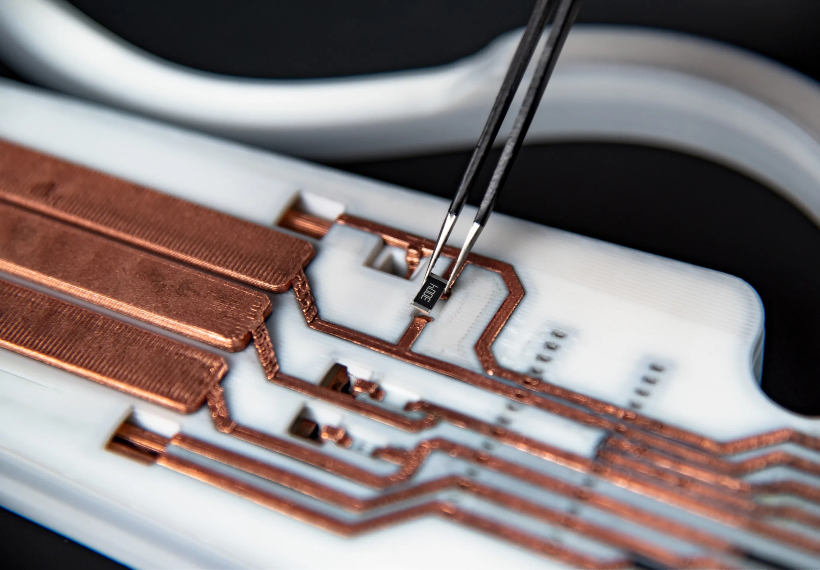
The core mechanism of Intercircuit is to construct an internal conductive path together with an adjacent cavity structure inside the object. We first print low-conductivity internal trajectories using conductive PLA, then generate cavities alongside these paths so that plating solution can reach the interior, while also adding vent structures to release trapped bubbles and clamping tabs for electrical connection during plating. During electroplating, the conductive PLA acts as the cathode and copper serves as the anode, allowing copper ions to deposit along the internal trajectories and transform the originally high-resistance printed paths into low-resistance, high-performance internal 3D circuits. The key idea is not merely plating the surface, but enabling plating to reach the interior through cavities so that complex spatial circuits can also be enhanced.
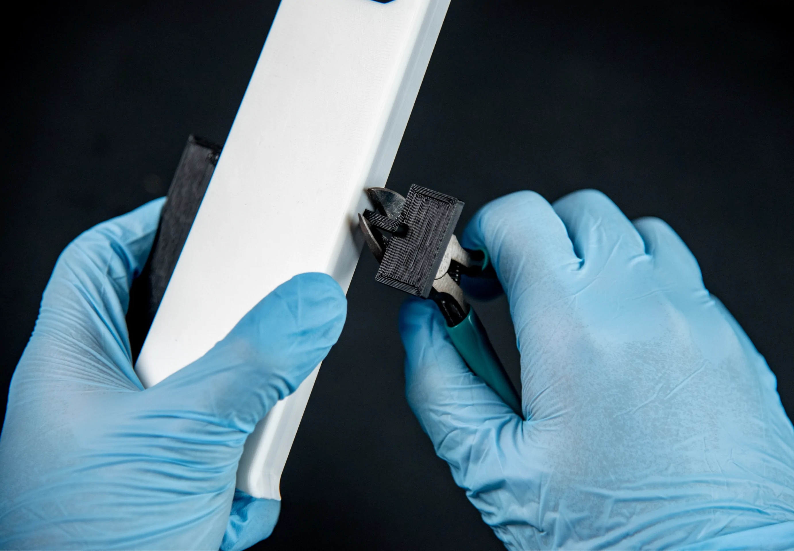
Fabrication
The fabrication process consists of a continuous sequence from design to final assembly. We first import the base model into Rhino / Grasshopper and manually define spatial polylines that represent the internal conductive paths. With the help of our design tool, these polylines are converted into printable conductive trajectories, adjacent cavities, clamping structures, and vent holes. The object is then fabricated through multi-material FDM printing; in our implementation, we used a consumer-grade Bambu Lab X1 printer with regular PLA and commercially available conductive PLA. After printing, the part is placed in a copper electroplating solution for selective plating. To avoid trapped air inside the cavities, we flush the interior with a syringe and maintain continuous stirring during the plating process. Finally, the clamping structures are removed, and electronic components are inserted or soldered to complete the assembly. This pipeline integrates internal 3D circuit design, selective electroplating enhancement, and final interactive object assembly into one reproducible workflow.
Evaluation
We conducted a systematic evaluation of the geometry and fabrication stability of the internal conductive structures, and organized the results into reusable design guidance. First, in the test of conductive path and cavity cross-sectional area, we fixed the conductive trajectory at 3 mm × 3 mm and varied the cavity size. The results showed that for a 100 mm internal plated path, the resistance became stable once the cavity cross-sectional area exceeded 4.8 mm². Second, in the turning-angle test, we compared different internal turning geometries and found that turns close to 90° offered a better balance between conductivity and spatial efficiency. We also evaluated bending complexity in the same plane and bending complexity in three-dimensional space. The results showed that adding vent holes reduced the time needed for complete plating, and that even under more complex spatial routing, the plated samples still achieved stable low resistance, with multiple 3D test pieces measuring below 0.5 Ω. Together, these evaluations show that Intercircuit not only enables internal conductive structures, but also provides concrete geometric guidelines for designing complex 3D circuits.
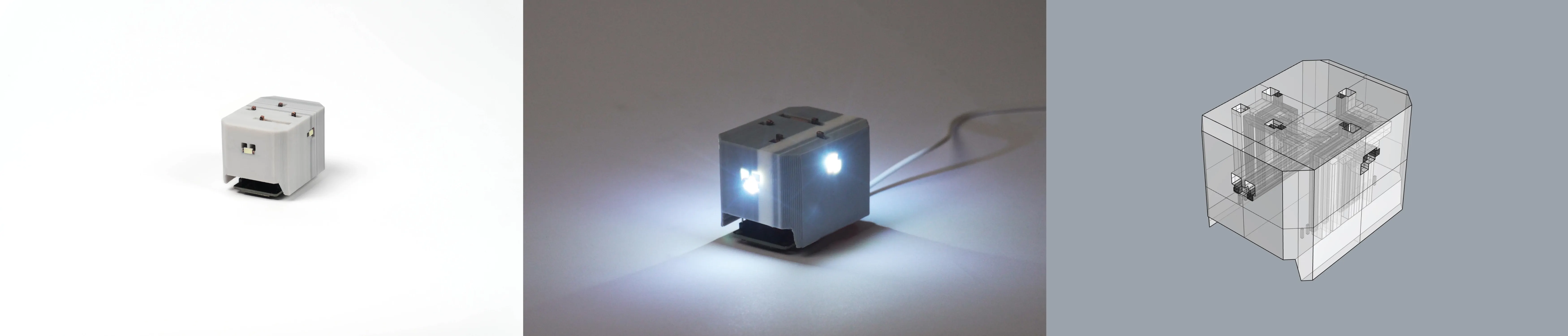
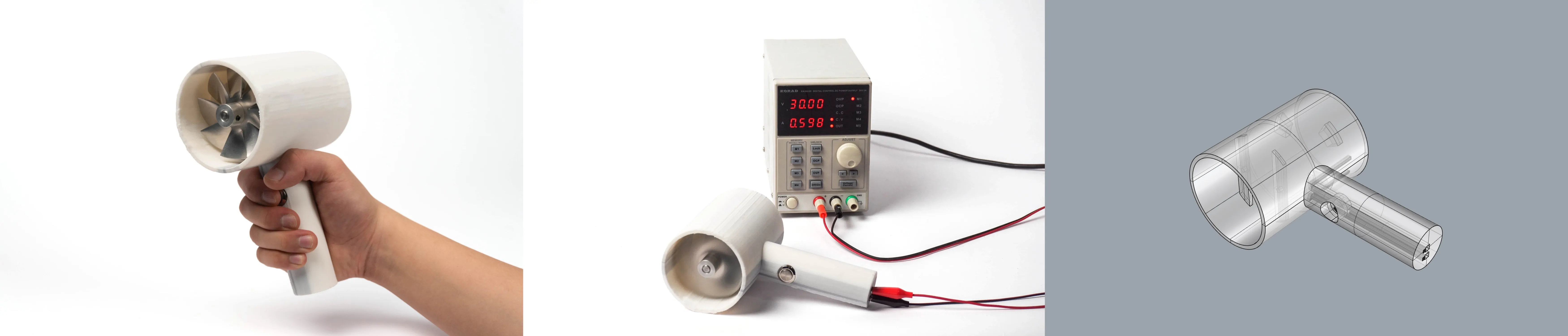
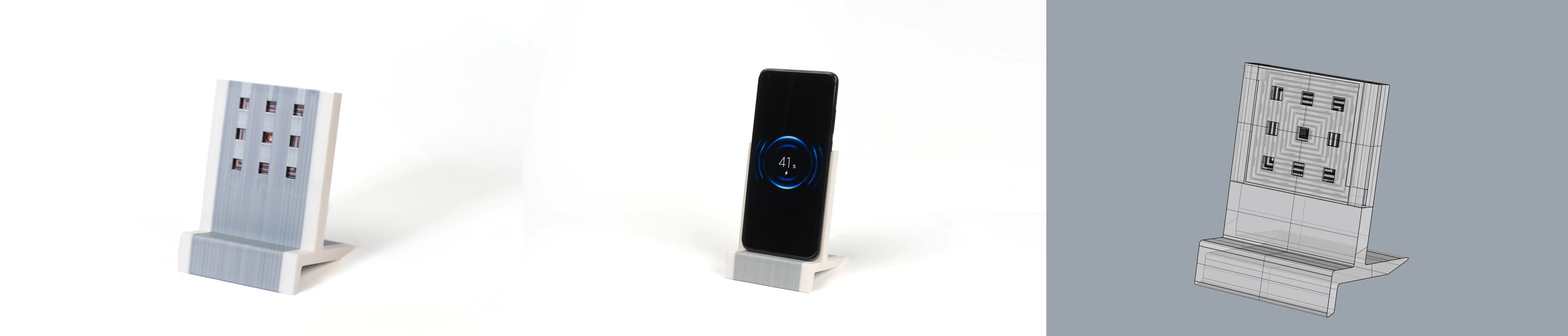
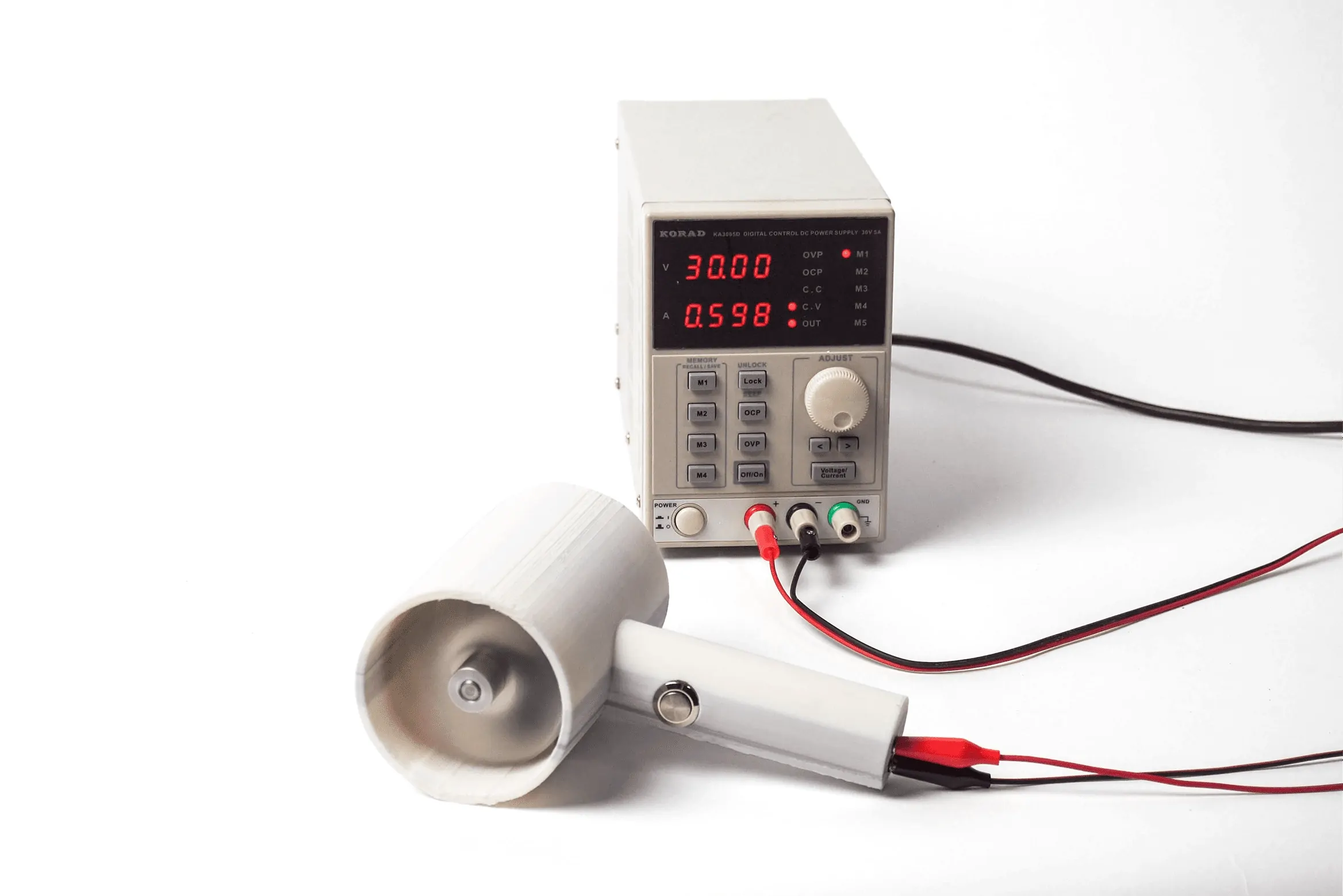
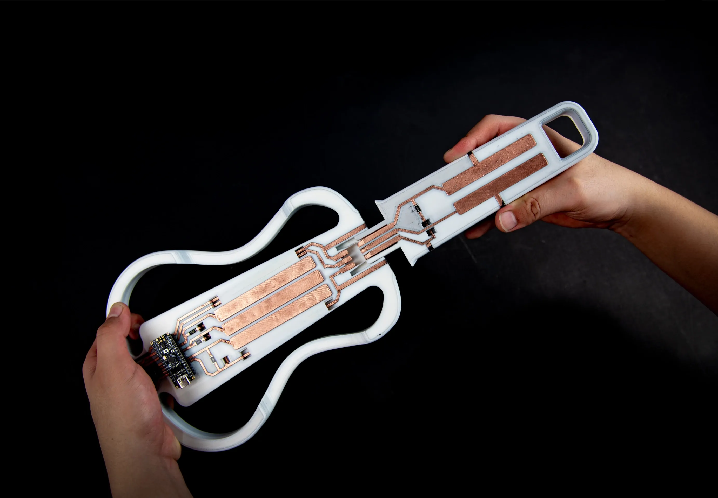
Applications
We demonstrate Intercircuit through three applications that reflect different directions of interactive fabrication. Together, these three cases demonstrate the method’s value in complex spatial circuitry, high-power applications, and functional enhancement of everyday objects.