
The advent of conductive thermoplastic flaments and multi-material 3D printing has made it feasible to create interactive 3D printed objects. Yet, challenges arise due to the volume constraints of desktop 3D printers and the high resistive characteristics of current conductive materials, making the fabrication of large-scale or highly conductive interactive objects can be daunting. We propose E-Joint, a novel fabrication pipeline for 3D printed objects utilizing mortise and tenon joint structures combined with a copper plating process. The segmented pieces and joint structures are customized in software along with integrated circuits. Then electroplate them for enhanced conductivity. We designed four distinct electrifed joint structures in the experiment and evaluated the practical feasibility and efectiveness of fabricating pipes. By constructing three applications with those structures, we verifed the usability of E-Joint in making large-scale interactive objects and showed the path to a more integrated future for manufacturing.
Background
Desktop 3D printing has greatly expanded the possibilities of interactive prototyping, yet large-scale interactive objects still face two major constraints. First, once an object exceeds the printer’s build volume and must be segmented, it becomes difficult to maintain both stable physical connections and electrical connections. Second, current conductive printing materials remain highly resistive, while existing selective electroplating methods are mostly limited to outer surfaces, making it difficult to support higher-load, safer, and more complex three-dimensional circuits. E-Joint was developed to unify assembly and electrical continuity within the same connection structure.
Method Overview
E-Joint combines mortise-and-tenon structures, conductive traces, and copper electroplating into one workflow so that segmented parts can achieve mechanical locking and electrical continuity at the same time. The method brings together three connected parts:
- a fabrication pipeline for electroplating-enhanced electrified joints
- a parametric design editor for segmentation, joint generation, and circuit integration
- performance evaluation and application validation across different joint and object types
Mechanism
E-Joint integrates structure and conductivity into the same interface. Each electrified joint serves as both a physical connector and an electrical pathway, reducing the need for additional fasteners, wires, or post-assembly electronics.
Electrified joint
We designed four types of electrified joints for different connection scenarios. Together, they form a structural vocabulary ranging from high-strength fixed joints to replaceable modular interfaces.
- (a)The straight joint provides the most direct and stable basic connection;
- (b)The dovetail joint offers stronger axial locking and is suited for locations requiring higher tensile and shear resistance;
- (c)The expansion joint introduces additional contact pressure through deformation and is better suited for multi-line electrical connections;
- (d)The spring-clip straight joint supports detachable and repeatedly pluggable modular connections.
Internal Circuits
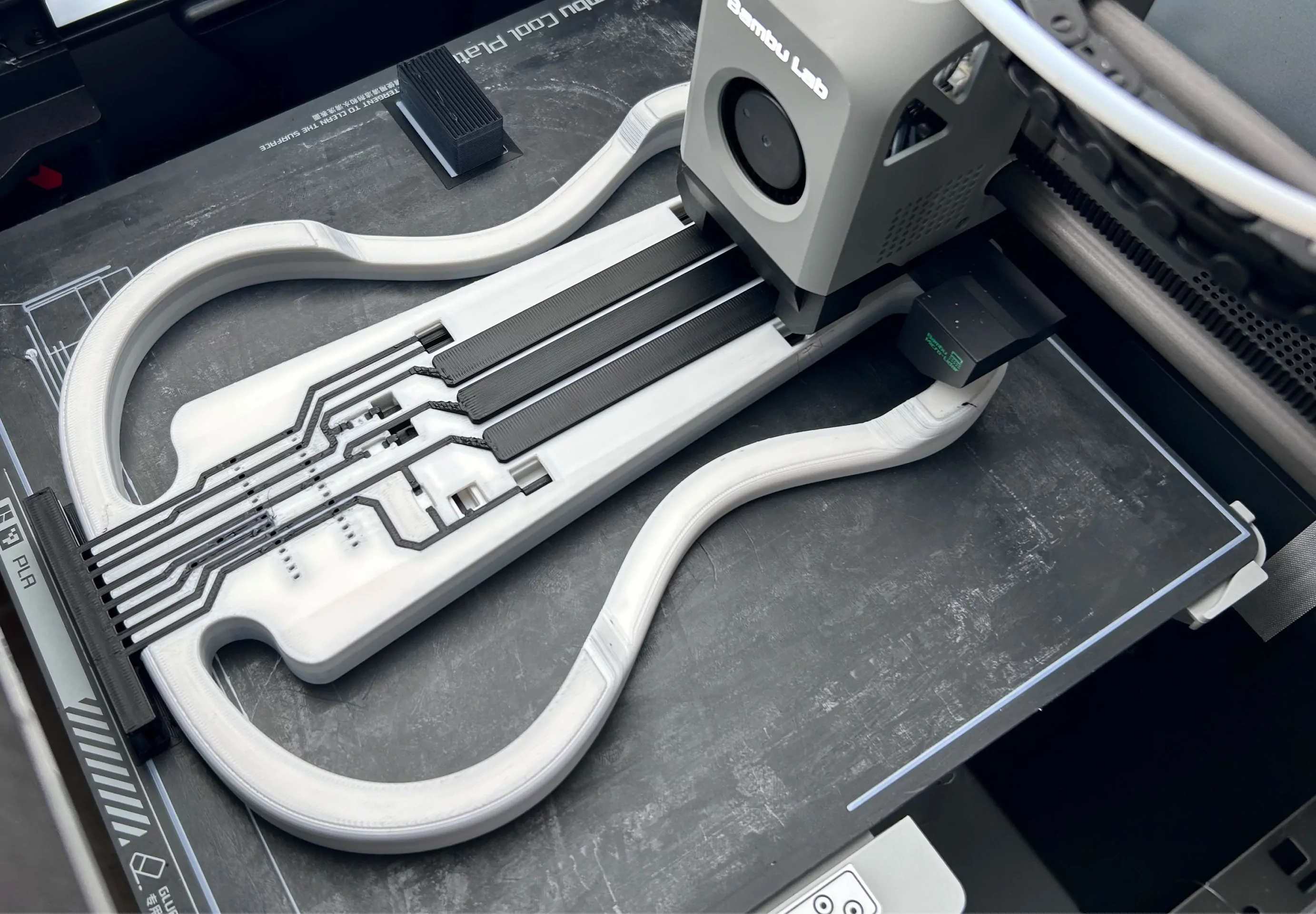
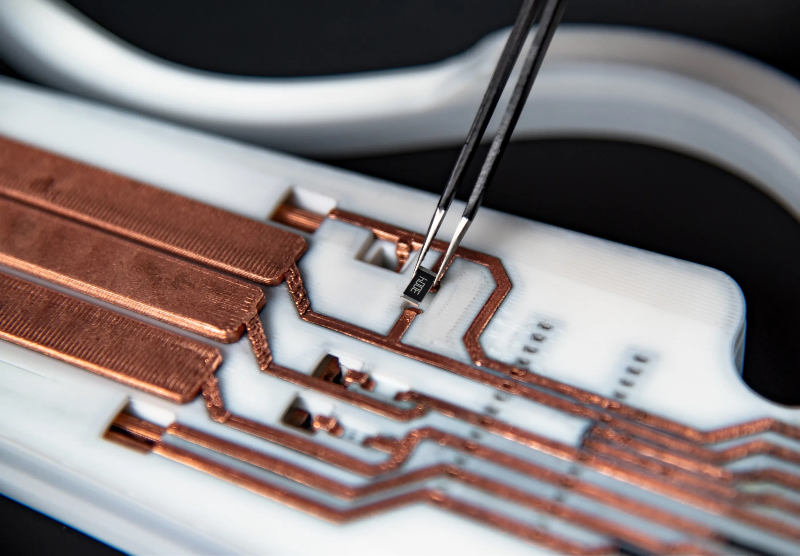
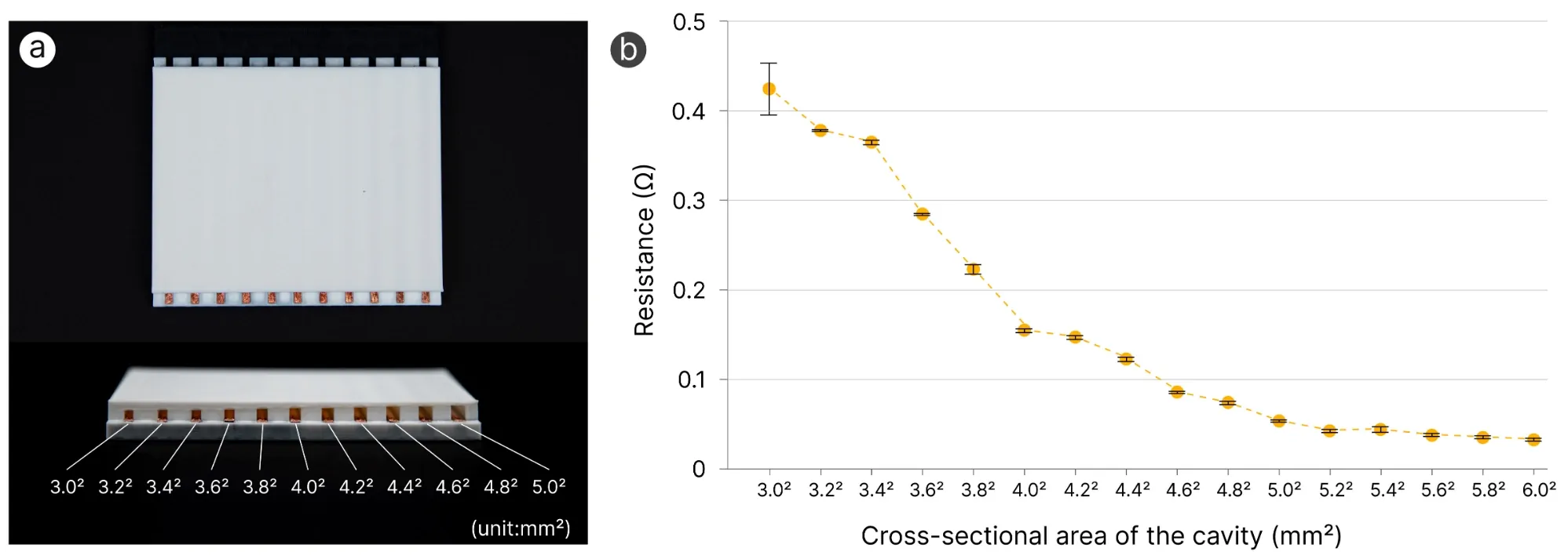
To support internal circuits, cavities are created around conductive PLA traces so that electroplating solution can reach the interior of the object. This converts high-resistance printed traces into low-resistance conductive paths and enables embedded electronic components inside large-scale 3D printed objects. A more detailed introduction to the internal circuitry is available in intercircuit. The workflow also generates two types of component slots: surface mount slots and pin slots, so that electronic components can be integrated directly into the printed structure.
Fabrication Pipeline
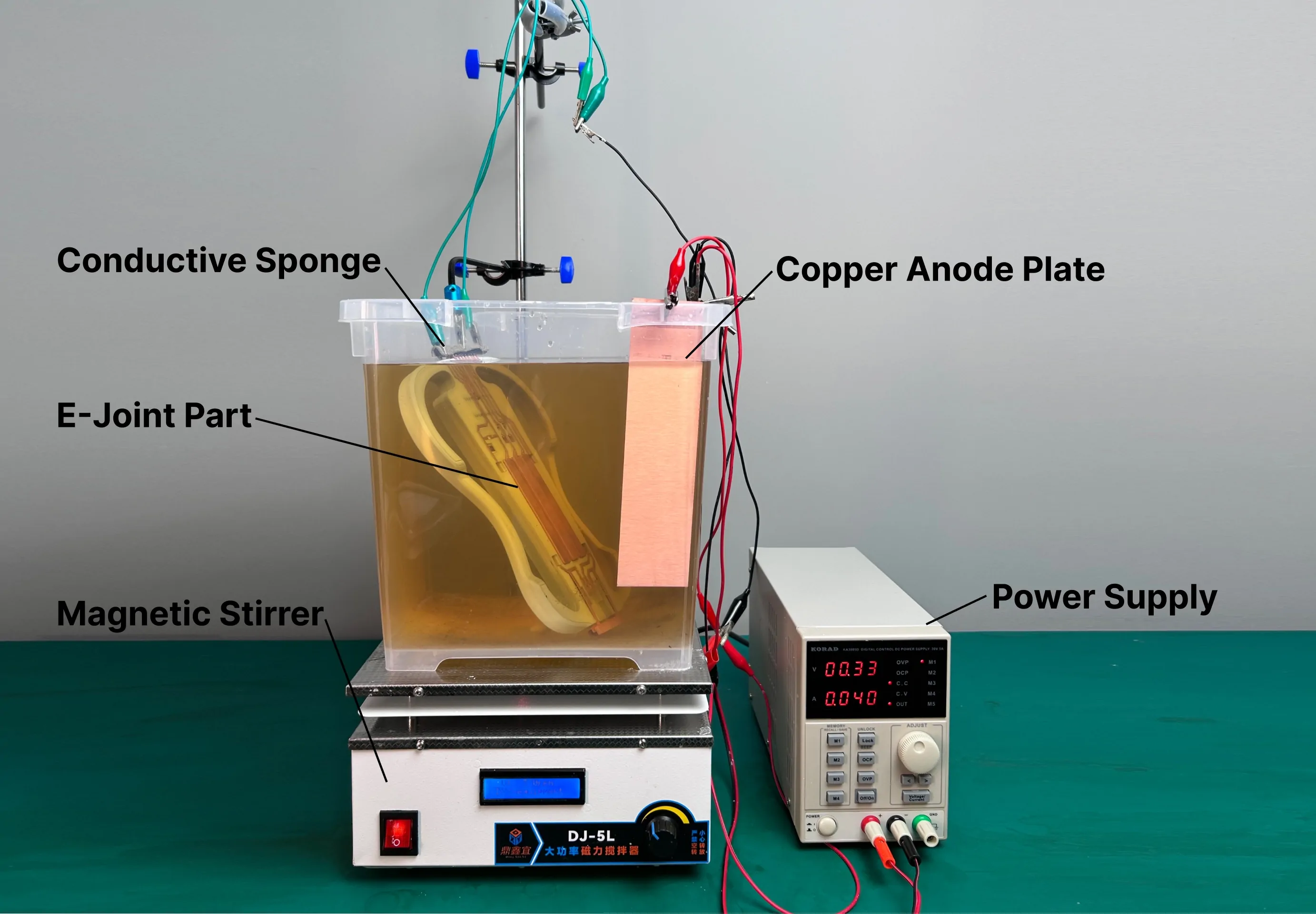
The full fabrication pipeline consists of five stages. We first use Rhino3D / Grasshopper to segment the model, generate joints, place components, and design either surface or internal circuits; we then fabricate the structural and conductive parts through multi-material FDM printing; after printing, the exposed conductive PLA regions are processed with copper electroplating; the parts then go through rinsing, passivation, drying, and protective finishing; finally, electronic components are inserted and the full object is assembled by insertion. This workflow integrates large-object segmentation and highly conductive interactive circuitry into one continuous personal fabrication method.
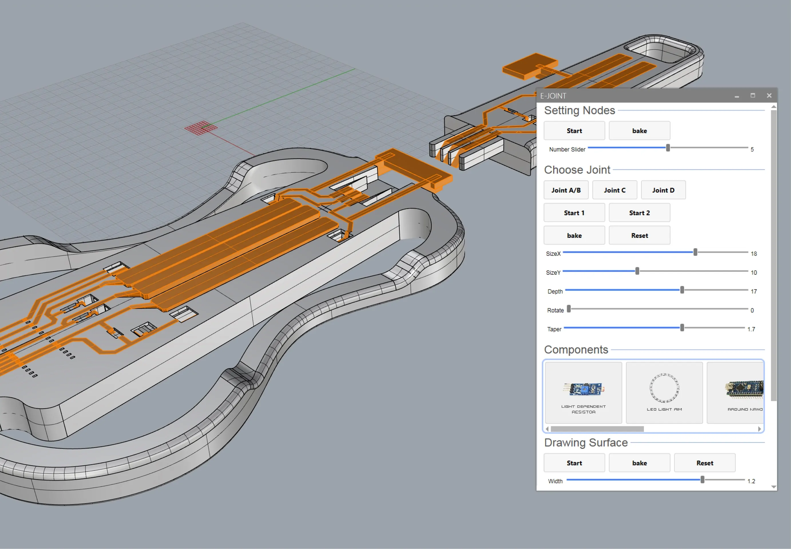
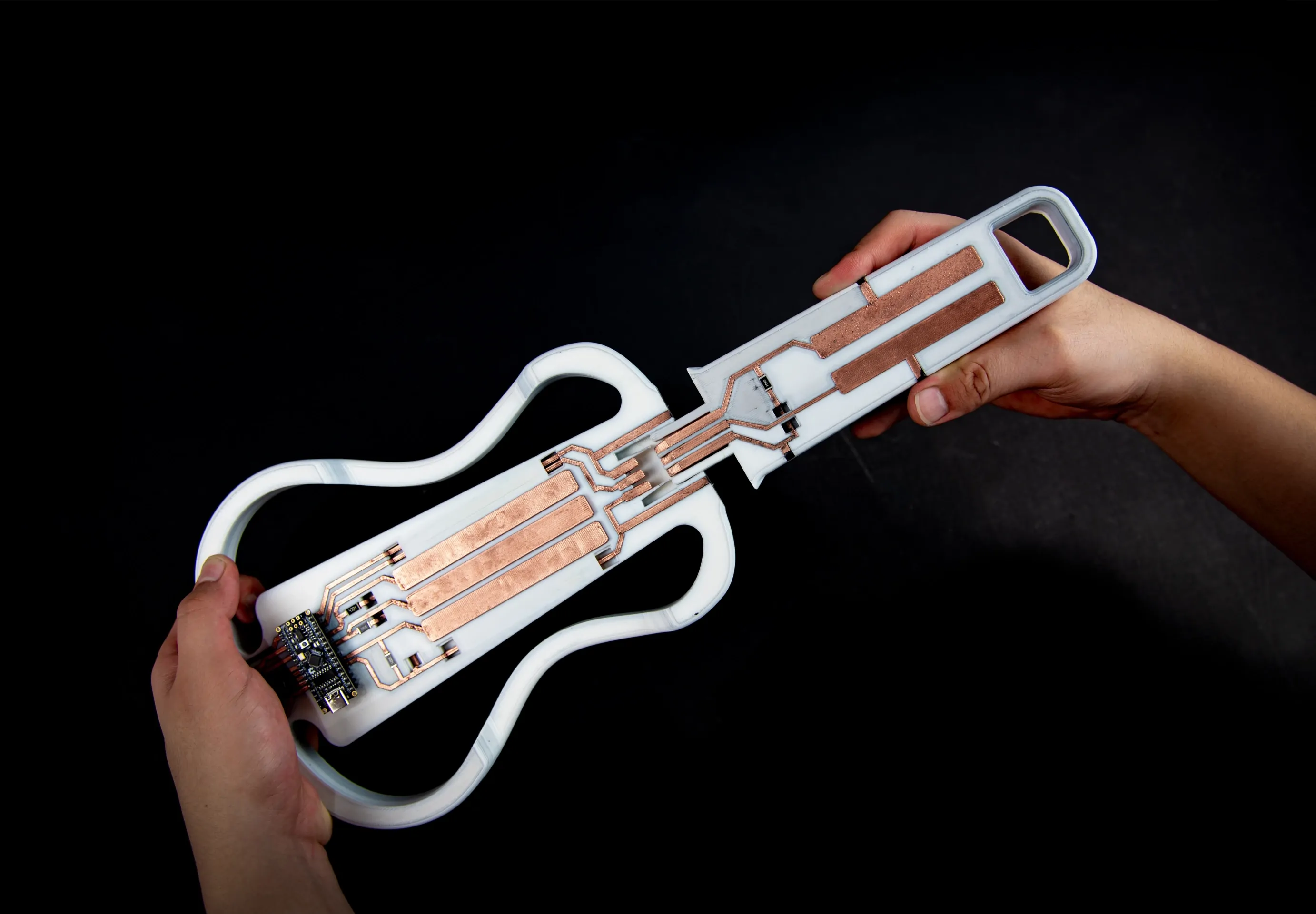
E-Joint Design Tool
We developed the E-Joint Design Editor to support the complete design workflow. Designers can import an original model, generate selectable grid points on contact surfaces, define joint positions, and let the system automatically perform Boolean operations. They can also place electronic components from a built-in library, draw surface or internal 3D Conductive PLA Traces, and automatically generate matching internal cavities and Clamp Plates. After design, the model can be exported in separate layers for structural and conductive materials. This brings structure, connection, and circuit design for large-scale interactive objects into a single parametric interface.
Guidelines
Design Guidelines
To balance structural stability and electrical performance, we derived a set of reusable design guidelines. A single mortise-and-tenon structure is recommended to have a total thickness of at least 20 mm, and a total width and length of at least 50 mm. A single conductive trace is recommended to be at least 3 mm wide and 4 mm thick, with spacing between adjacent traces of no less than 1 mm. For assembly tolerance, the straight joint, dovetail joint, and expansion joint are recommended at around 0.1 mm, while the spring-clip straight joint uses around 0.15 mm to better support repeated insertion and removal. In addition, we provide the characteristic parameters for each of the four Electrified joints.
Fabrication Guidelines
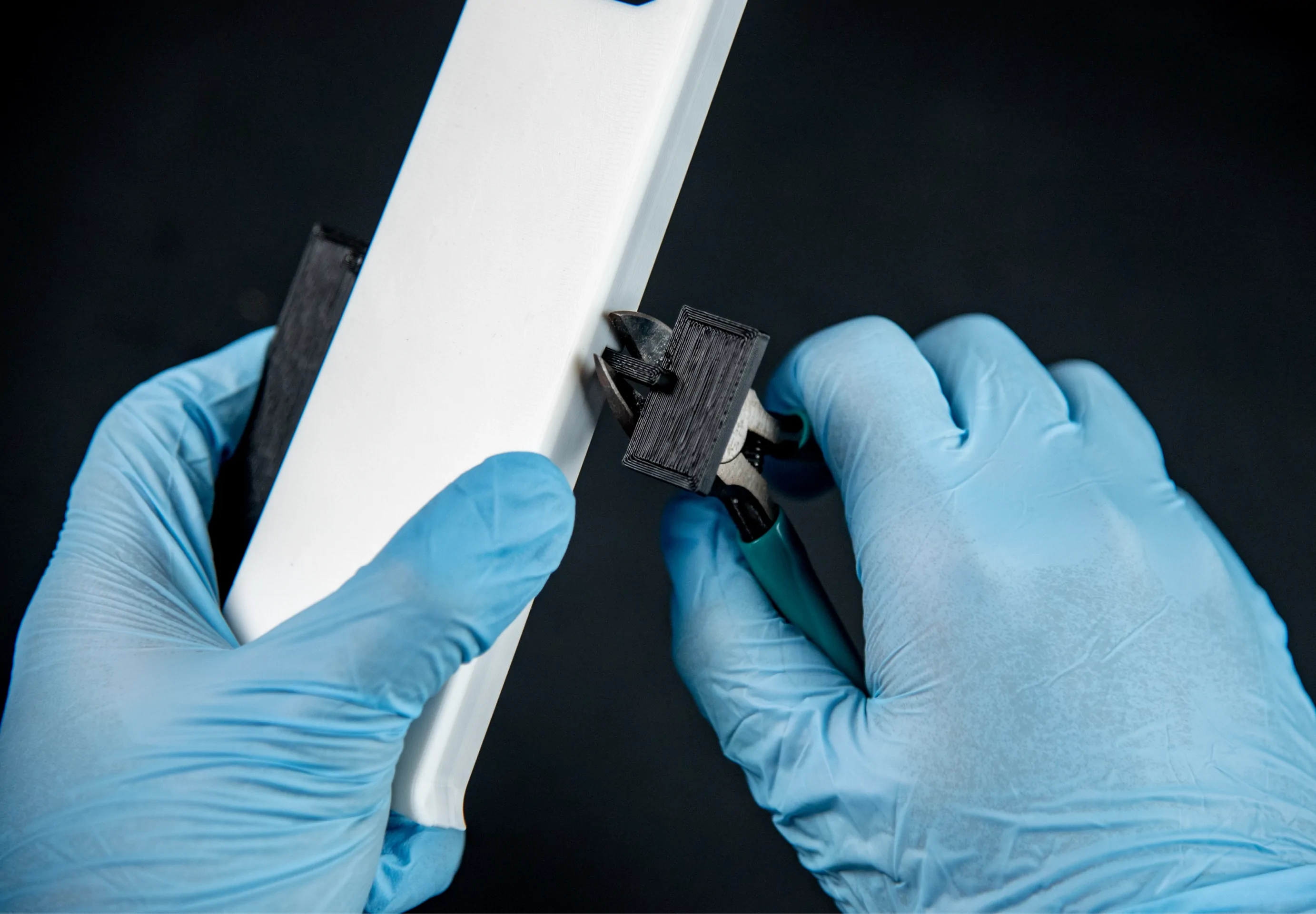
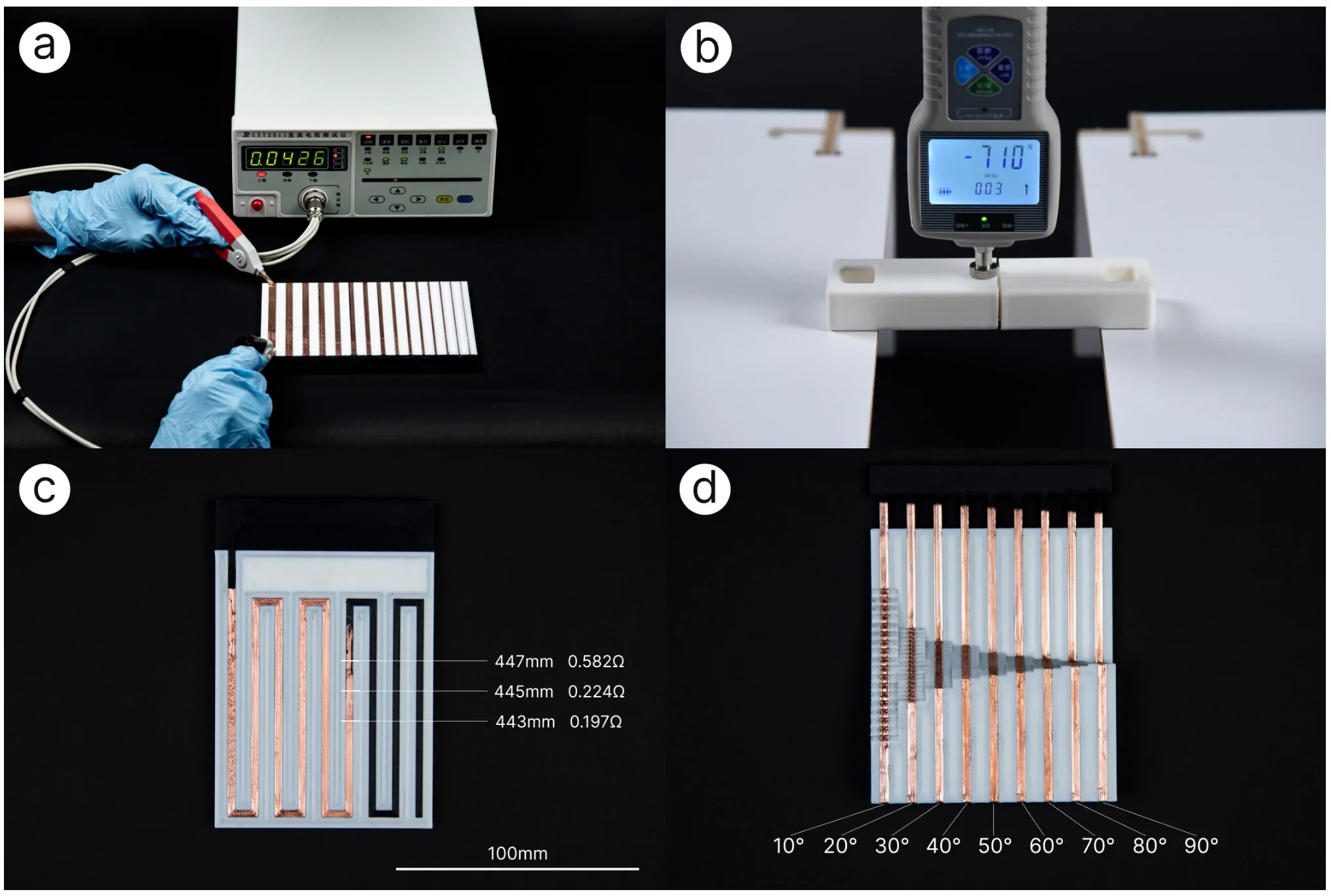
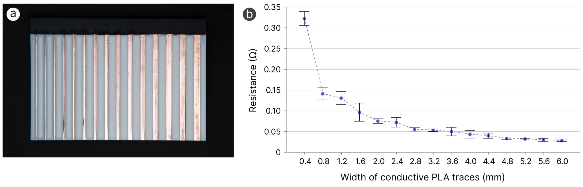
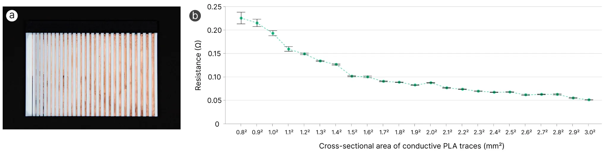
For fabrication, we use multi-material FDM printing to produce both structural and conductive parts. To reduce resistance between conductive PLA layers, we use 100% infill, a linear filling strategy, and more than 5 wall layers, while aligning the internal fill direction with the wiring direction as much as possible. After printing, the conductive PLA acts as the cathode during copper electroplating, a process that improves conductivity by roughly five orders of magnitude. In our setup, plating begins at 0.04 A to form an initial visible copper layer and then continues at 0.02 A for several hours to achieve more uniform deposition.
Evaluation
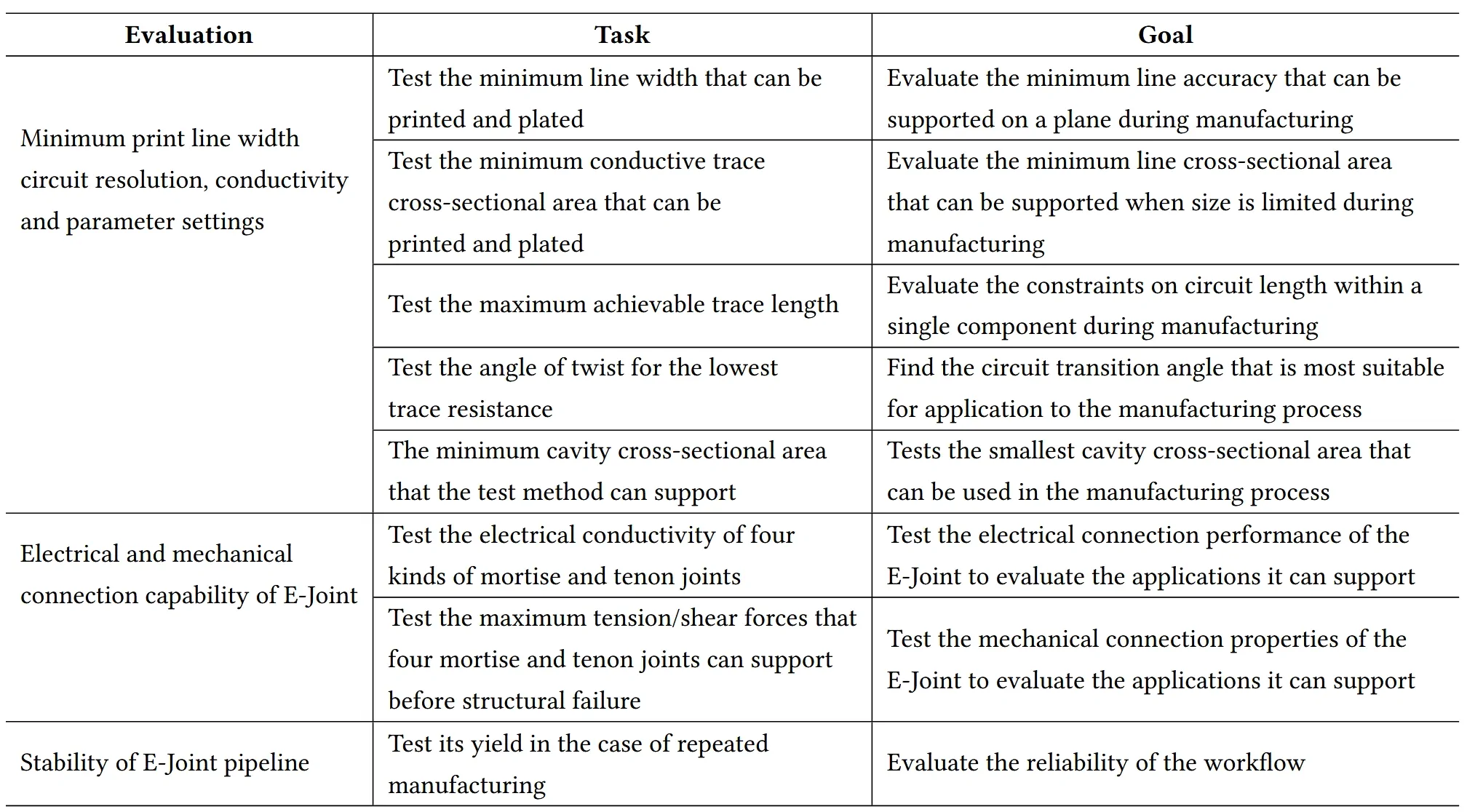
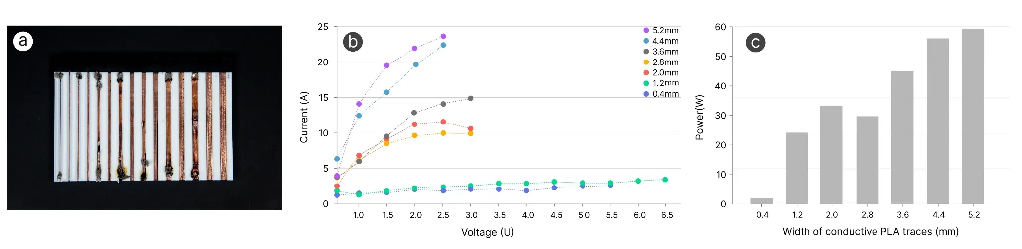
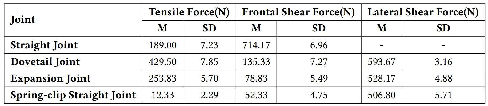
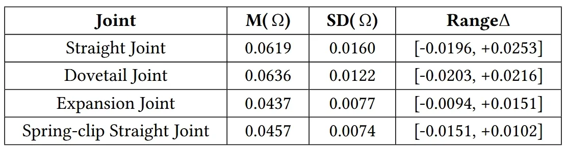
We evaluated the system in terms of conductivity, power handling, and mechanical connection performance. For line-width testing, we fabricated test pieces with a trace length of 100 mm, a depth of 3 mm, and widths ranging from 0.4 mm to 6.0 mm. After electroplating, four-probe measurements showed that traces with a width of 2.0 mm or more achieved stable conductivity with resistance below 0.1 Ω. For power testing, we continuously increased the voltage across the traces until failure; the 5.2 mm trace reached an instantaneous load of 58.625 W and tolerated a maximum current of about 23.45 A before burning out. For mechanical testing, we examined tensile and shear behavior across all four joint types, showing that different joints excel in different scenarios such as high-strength locking, multi-line connection, and repeated plugging, confirming that E-Joint is both electrically functional and structurally reliable in practice.
Applications
We demonstrate E-Joint through three applications operating at different scales and functional requirements.
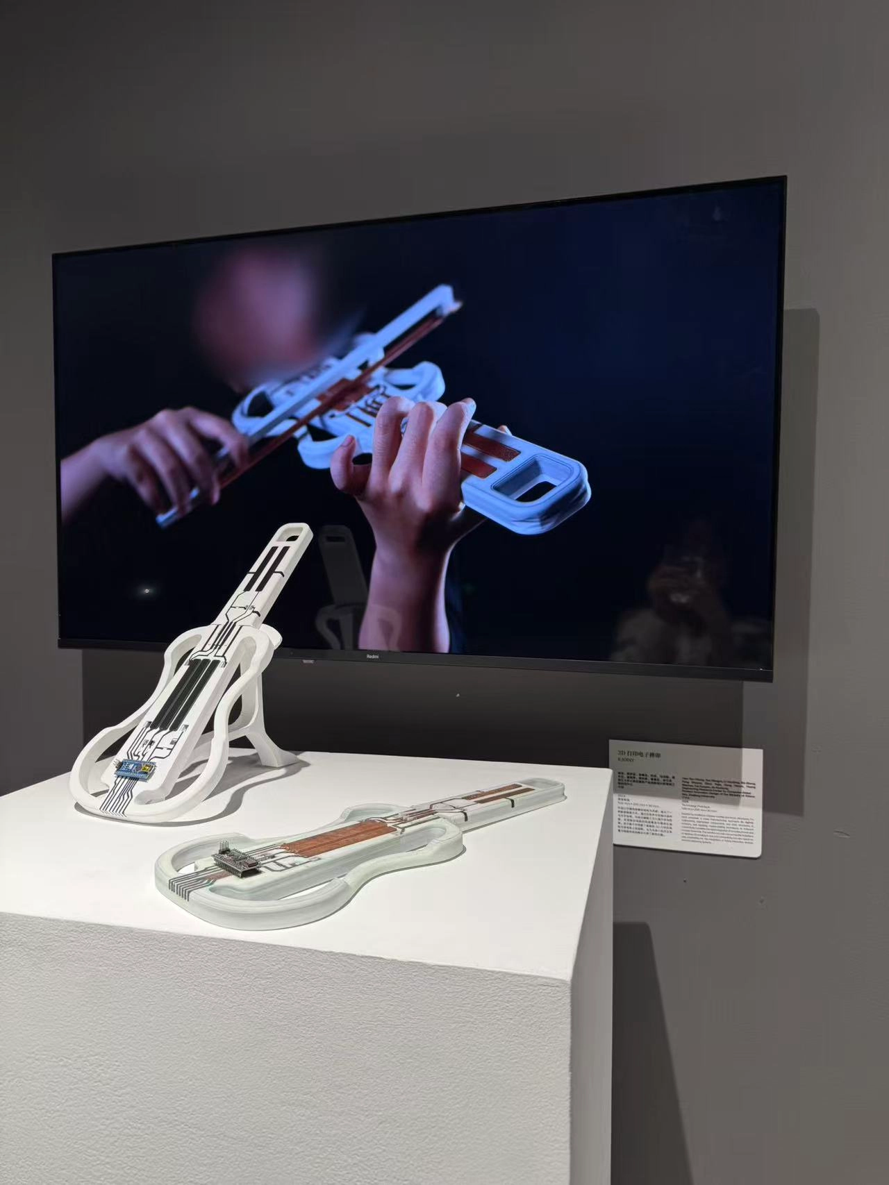
Exhibition (CHINA - HANGZHOU Art and Technology Biennale)